تحت الانشاء Under Construction
Description
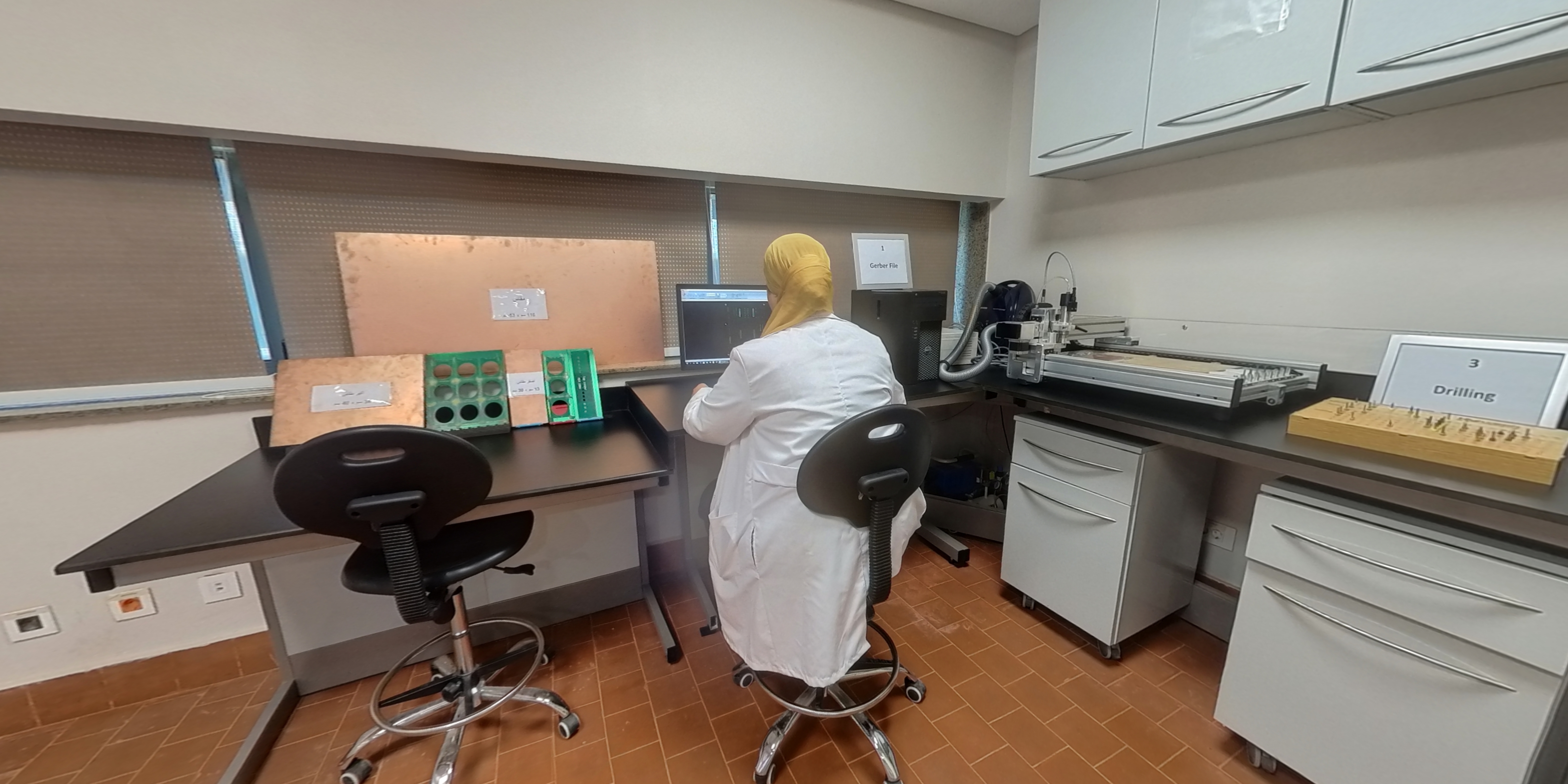
Moving the attractive electronic design of the connection paths from an electronic image (B file) (“Gerber”) to the stage of actual connections created from precise copper paths on a circuit that electrically connects the electronic components to each other.
The client targets the research client at the level of (research laboratories of the Electronic Research Institute - university education sector, industrial education - research sector in industrial companies - in addition to individuals).
The R&D client is considered to be of the following nature:
Limited number of circles - small circle sizes - repetition of experiments)
Which means that factories with mass production technology are unable to meet the nature of these requests, which are limited in number or small manufacturing sizes, as they are considered a restriction on their production movement. It also reduces the waste of time and cost of the customer for manufacturing abroad and adds air freight that is greater than the manufacturing cost.
Therefore, the laboratory's technology enables it to deal with the small number/sizes of these circuits.
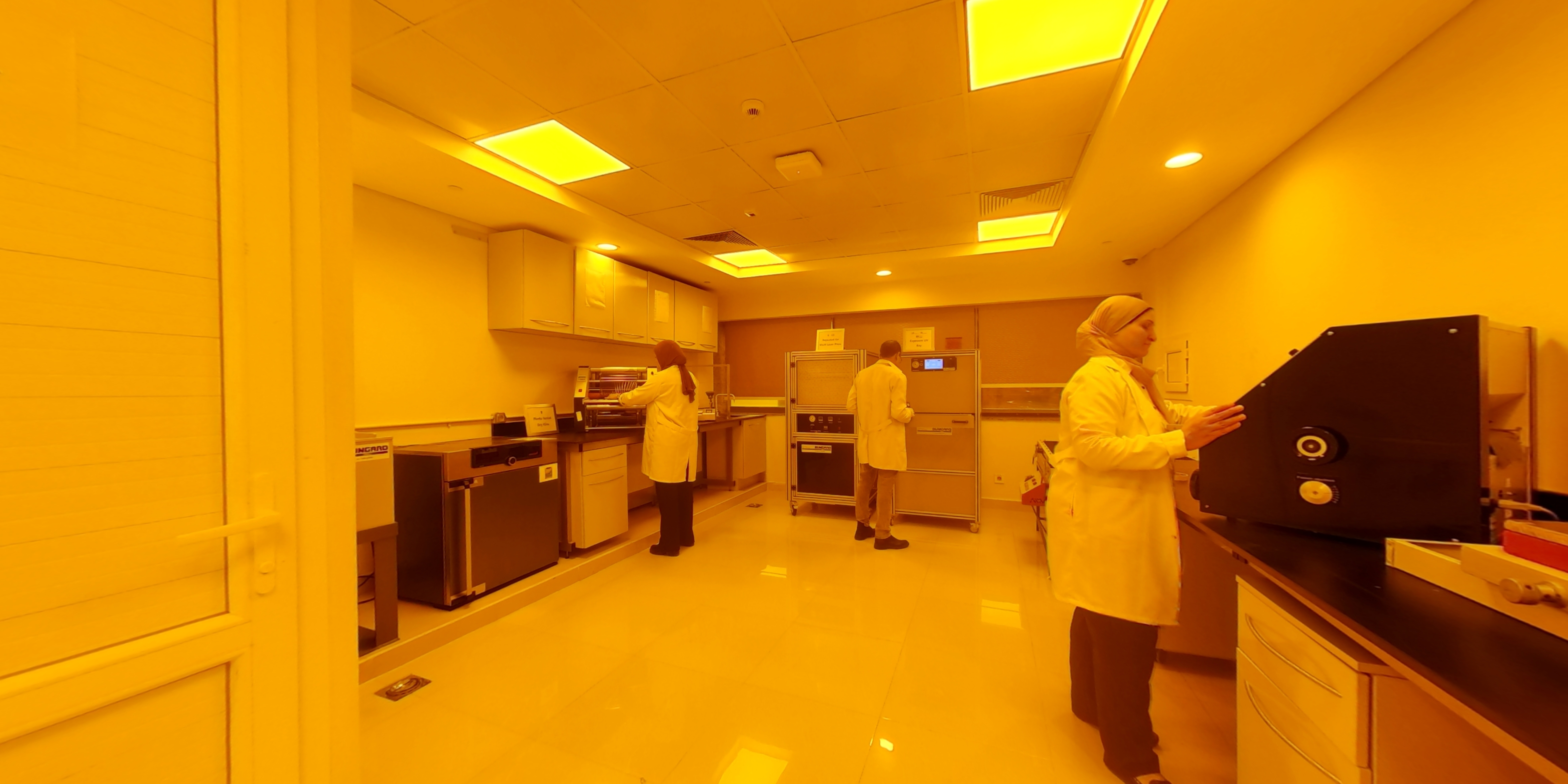
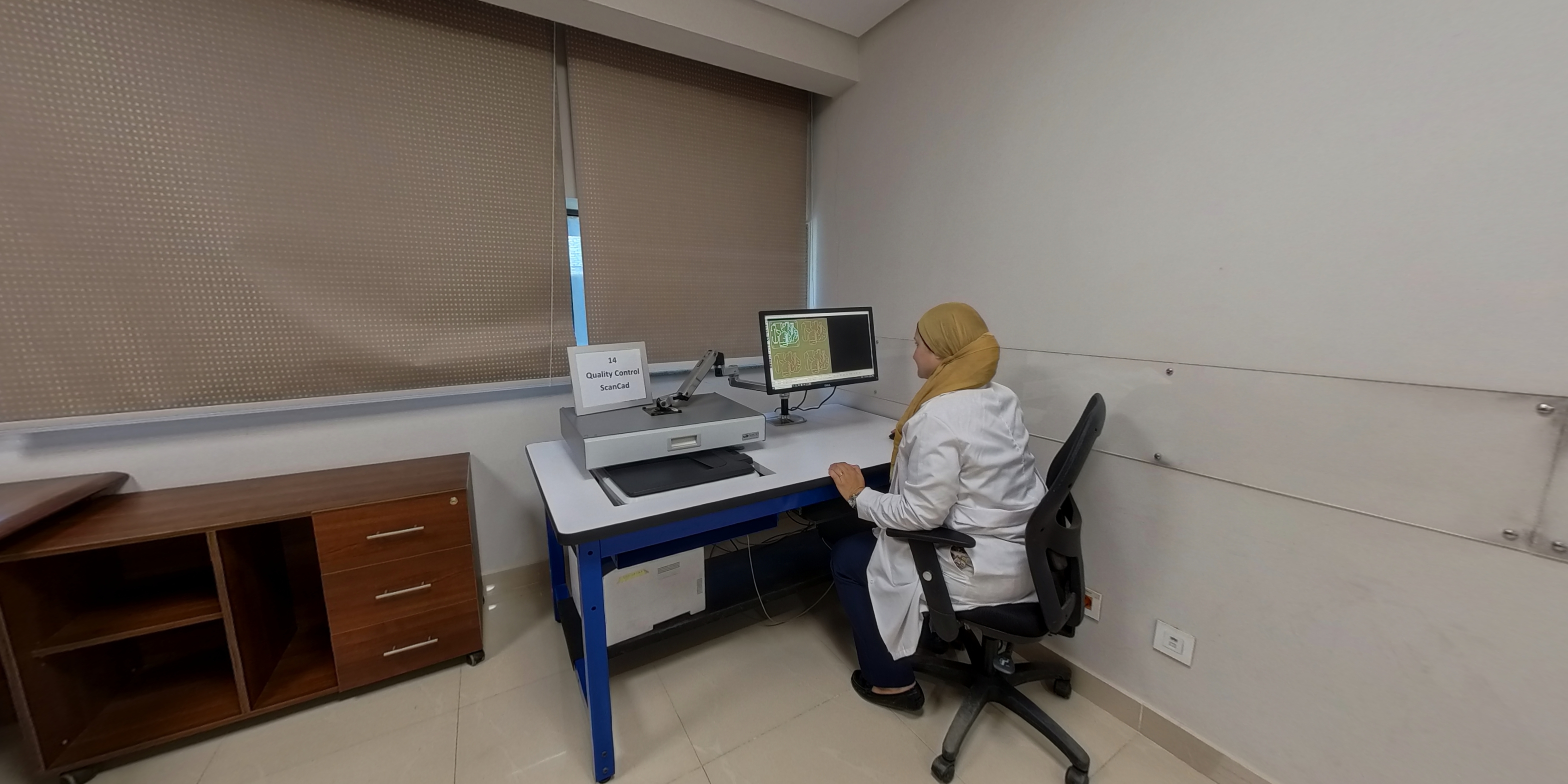
The lab manufactures printed circuits:
- With an accuracy of up to 0.15 mm for both (the width of the connection paths/and the interspaces between them).
- The diameter of the connection holes between the layers is 0.3 mm.
- Manufacturing circuits with (one layer - two layers - multi-layers up to 6 layers),
- The maximum manufacturing size of printed cards reaches (30 cm x 40 cm).
Lab Contents


